
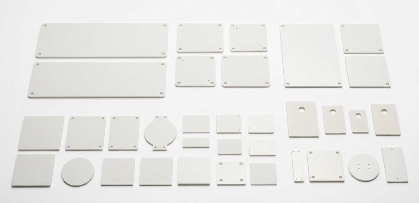
Custom Aluminum Nitride (AlN) Ceramic Components

The ultimate thermal management material. Combining ultra-high thermal conductivity (>170 W/m·K) with excellent electrical insulation. We deliver precision-machined AlN components and substrates tailored for power electronics, semiconductors, and high-power optoelectronics. Custom micro-machining and metallization to your drawings.

Precision-Graded AlN to Match Your Thermal Demands

Not all thermal challenges are equal. We provide Aluminum Nitride in various grades, optimized for both thermal performance and manufacturing scale, ensuring you get the exact heat dissipation your project requires.

Properties of

Property (Unit)Testing StandardTypical Grade (AlN-170)High Thermal Grade (AlN-200)
Density (g/cm³)DIN EN 623-2≥ 3.20≥ 3.30
Vickers Hardness (HV₁₀)DIN EN 843-41000 - 11001000 - 1100
Flexural Strength (MPa)DIN EN 843-1300 - 350350 - 400
Compressive Strength (MPa)DIN EN 843-12000 - 25002000 - 2500
Young's Modulus (GPa)DIN EN 843-2310 - 330310 - 330
Thermal Conductivity (W/(m·K))DIN EN 821-2170 - 180200 - 230
Coefficient of Thermal Expansion (10⁻⁶/K)DIN EN 821-14.5 (Matches Silicon)4.6 (Matches Silicon)
Specific Heat Capacity (J/(kg·K))/740740
Max. Operating Temp. (In Air) (°C)/1000 °C1000 °C
Max. Operating Temp. (Inert/Vacuum) (°C)/1900 °C1900 °C
Dielectric Strength (kV/mm)DIN EN 60672-215 - 1815 - 18
Dielectric Constant (1 MHz)/8.8 - 9.08.5 - 8.8
Volume Resistivity (Ω·cm, 20 °C)/> 10¹⁴> 10¹⁴

Beyond Raw Materials: Advanced AlN Processing

Aluminum Nitride is notoriously brittle and difficult to process. Our audited facilities utilize green-state machining, laser technology, and advanced brazing to deliver ready-to-assemble components.

⚡ Metallization & Brazing (DBC / AMB / Thin Film): We supply AlN substrates with Direct Bonded Copper (DBC) or Active Metal Brazing (AMB) for power electronics, as well as thin-film sputtering (Au/Pt/Ti) for RF applications.

🎯 Laser Micro-Machining & Scribing: Achieving complex via holes (down to 0.1 mm), precise edge profiling, and laser scribing for snap-apart LED substrates without inducing micro-cracks.

💎 Ultra-Flat Polishing: Surface lapping and mirror polishing to achieve extreme flatness and surface roughness of Ra < 0.05 μm, critical for direct die attach and wafer bonding.

Thermal Solutions for High-Density Technologies

The Challenge: Silicon Carbide (SiC) and Gallium Nitride (GaN) chips generate massive localized heat. Traditional Al<sub>2</sub>O<sub>3</sub> substrates cause thermal bottlenecks.

Solution: AMB/DBC AlN Substrates quickly spread the heat load, lowering junction temperatures, extending component life, and increasing power density in electric vehicles and high-speed railways.

The Challenge: Wafer processing requires perfect thermal uniformity and a material that expands at the exact same rate as the Silicon wafer to prevent sliding and defect generation.

Solution: High-Purity AlN Heaters and Chucks. With a CTE of 4.5 x 10⁻⁶/K (perfectly matching Silicon) and excellent halogen plasma resistance, it ensures defect-free wafer yields.

The Challenge: Heat degradation is the #1 killer of high-power UV-LEDs and telecom laser diodes.

Solution: Metallized AlN Submounts. Acting as an immediate heat sink, these submounts ensure wavelength stability and prolong the lifespan of high-frequency optical communication modules.

Quality Controls for Your Thermal Components

💎 Strict Flatness & Thickness Tolerance Checks.
📦 Flexible MOQ for Prototype Validation.

Scroll to Top